WS2812 – Non-Blocking Algorithm
- J Fowler
- Jun 28, 2022
- 4 min read

Updated: Jun 30, 2022
By: JFowler June 28, 2022
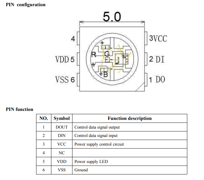
WS2812 is an addressable Red-Green-Blue (RGB) Light-Emmitting Diode (LED) integrated circuit (IC). The pin count may vary, however, the four primary pins include: 5V Power Supply, Ground, Data-In, and Data-Out. Several WS2812 nodes may be connected in series. The Data-In of the first node is connected to the host CPU. Additional nodes can then be added by connecting the Data-Out of the last node in series to the Data-In of the newly appended node. This allows the user to control a myriad of RGB LEDs with a single CPU pin!
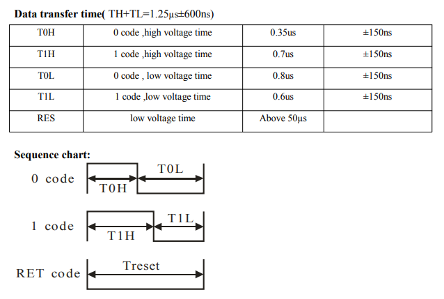
The WS2812 protocol is a series of 3-byte groups representing the Green, Red, and Blue color intensities. The first 3-bytes are captured by the first WS2812 node, the next 3-bytes by the second node, and so on and so forth. Each transmitted bit is comprised of a High Voltage Time followed by a Low Voltage Time.
(Diagrams from WS2812 Datasheet. https://cdn-shop.adafruit.com/datasheets/WS2812.pdf)
A commonly practiced WS2812 protocol implementation involves bit-banging a General-Purpose-Input-Output (GPIO) pin, connected to the Data-In of the first LED node, and delaying between GPIO voltage transitions. Since the High and Low times are relatively short, it is not practical, or possible, to leave the protocol handling algorithm between GPIO toggles. Instead, a series of “NOP” instructions are executed (the processor blocks and wastes away cycles) until the time comes to toggle the GPIO. This is not a terrible approach when working with only a few nodes, but it can quickly become troublesome with several nodes. Note from the data transfer time table that each bit-code requires between 1.05 to 1.4 microseconds. Each LED node will receive 24-bits which will take up to (1.4 us * 24) = 33.6-microseconds. With only 30-nodes, the algorithm would require over 1-millisecond to complete and the rest of the tasks on the device would be blocked – this is not acceptable for many applications.
Consider the WS 2812 93-LED wheel with all LED nodes connected in a single series. ( https://www.dfrobot.com/product-2091.html ) To successfully operate all 93-nodes, while still allowing the CPU to continue servicing its other non-blocking peripherals, a non-blocking solution for the WS2812 protocol is needed.

Theory -
The bit-code high and low voltage times allow for 150-nanoseconds of wiggle room each for a total of 0.3-microseconds. This flexibility allows for a common bit-code period, say 1.3-microseconds, for both the 1-bit and 0-bit codes. A hardware timer may be configured on the host CPU with the 1300-nanosecond period (the clock ticks up for 1300-nanoseconds and then resets to 0 and begins again). The timer is further configured to toggle an output compare (OC) pin when the tick value is equal to the value stored in the timer compare register. A Direct Memory Access (DMA) module may then be configured to automatically load the timer compare register with the next compare value. With this methodology, the application code only needs to fill the DMA buffer before the start of each new animation; the hardware takes care of the rest.
Each slot in the DMA buffer is filled with only one of three values:
0 – Toggle the OC pin high at the start of each new period.
bit0_tick – Toggle the OC pin low after the required high voltage time passes for a 0-bit code.
bit1_tick – Toggle the OC pin low after the required high voltage time passes for a 1-bit code.
Pseudo code for loading the DMA buffer is as follows:
N = 0
For each WS2812 LED
    For each byte (3-bytes per LED)
        For each bit (8-bits per byte)
            if bit is 1
                DMA_Buffer[N] = bit1_tick_value
            else
                DMA_Buffer[N] = bit0_tick_value

            N++
            DMA_Buffer[N] = 0
            N++
One shortcoming of this approach includes a relatively large data memory resource allocation. Each RGB LED is composed of 3-bytes or 24-bits. Each bit requires either a 16-bit or 32-bit slot in the DMA buffer. Thus, with 93-LEDs the DMA buffer could be up to (93 * 24 * 4) = ~9KB in length.
Application -
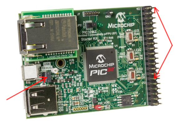
A Microchip PIC32MZ Starter Kit board (https://www.microchip.com/en-us/development-tool/dm320007) was configured with Microchip’s MPLabX Integrated-Development-Environment (IDE) and Harmony3 tool. (Harmony3 provides a useful Graphical-User-Interface (GUI) for enabling and configuring different hardware peripherals available on the CPU.) A hardware timer was set with a 1:1 prescaler value of the internal peripheral clock (100MHz) and set to a period of 1300-nanoseconds (129-ticks). An output compare peripheral was linked to the hardware timer and the behavior on a compare event was configured to toggle a corresponding OC pin. The WS2812 93-LED wheel was prepared with all 93-LEDs in a single series. The Data-In of the head LED node was connected to the OC pin. The 5V and Ground pins of the wheel were also connected to the starter kit board (5V shorted to USB DEBUG jumper and Ground on pin 39 of J12).
The capture compare tick count for the high and low voltage times for the 0 and 1 bits were calculated based upon the time/tick ratio of 1300-nanoseconds to 12-ticks.
#define WS2812_0BIT_TIME_HIGH_nS 425U
#define WS2812_0BIT_TIME_LOW_nS 875U
#define WS2812_1BIT_TIME_HIGH_nS 700U
#define WS2812_1BIT_TIME_LOW_nS 600U
#define WS2812_TIMER_PERIOD_nS 1300U
#define WS2812_TIMER_PERIOD_TICKS 129U
bit0_ticks = (WS2812_0BIT_TIME_HIGH_nS * WS2812_TIMER_PERIOD_TICKS) / WS2812_TIMER_PERIOD_nS) + 0.5);
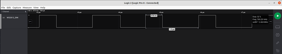
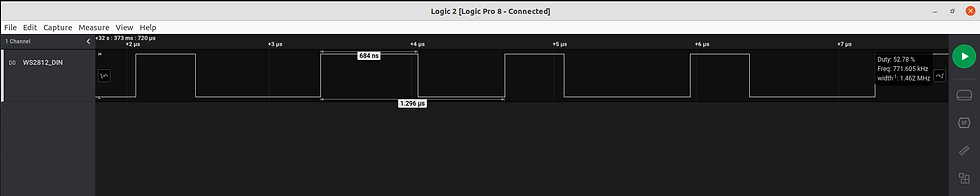
bit1_ticks = (WS2812_1BIT_TIME_HIGH_nS * WS2812_TIMER_PERIOD_TICKS) / WS2812_TIMER_PERIOD_nS) + 0.5);A Saleae Logic Analyzer (https://www.saleae.com/) was used to verify the high and low voltage times. Adjustments were made to the code-defined times as needed. The analyzer provided very clear and helpful feedback. I definitely recommend the analyzer to professionals, students, and enthusiasts alike. I have already used mine with other projects involving SPI and I2C communications and I have been very satisfied with its performance and utility. After a few adjustments, the high and low timings were found to be no more than 20-nanoseconds off.
A firework pattern was implemented in which each wheel section, starting at the center and working out, would light up and then slowly fade until off. The animation was rendered, converted to a GRB array, and finally converted to timer compare tick values and stored on the DMA buffer.

Conclusion -
The non-blocking algorithm for the WS2812 protocol worked very well. The 93-LED firework animation operated smoothly while simultaneously allowing other non-blocking tasks on the device to be serviced.
Comments